
The following are some of the frequently asked questions related to PN-Junction:
1. What is the need for doping?
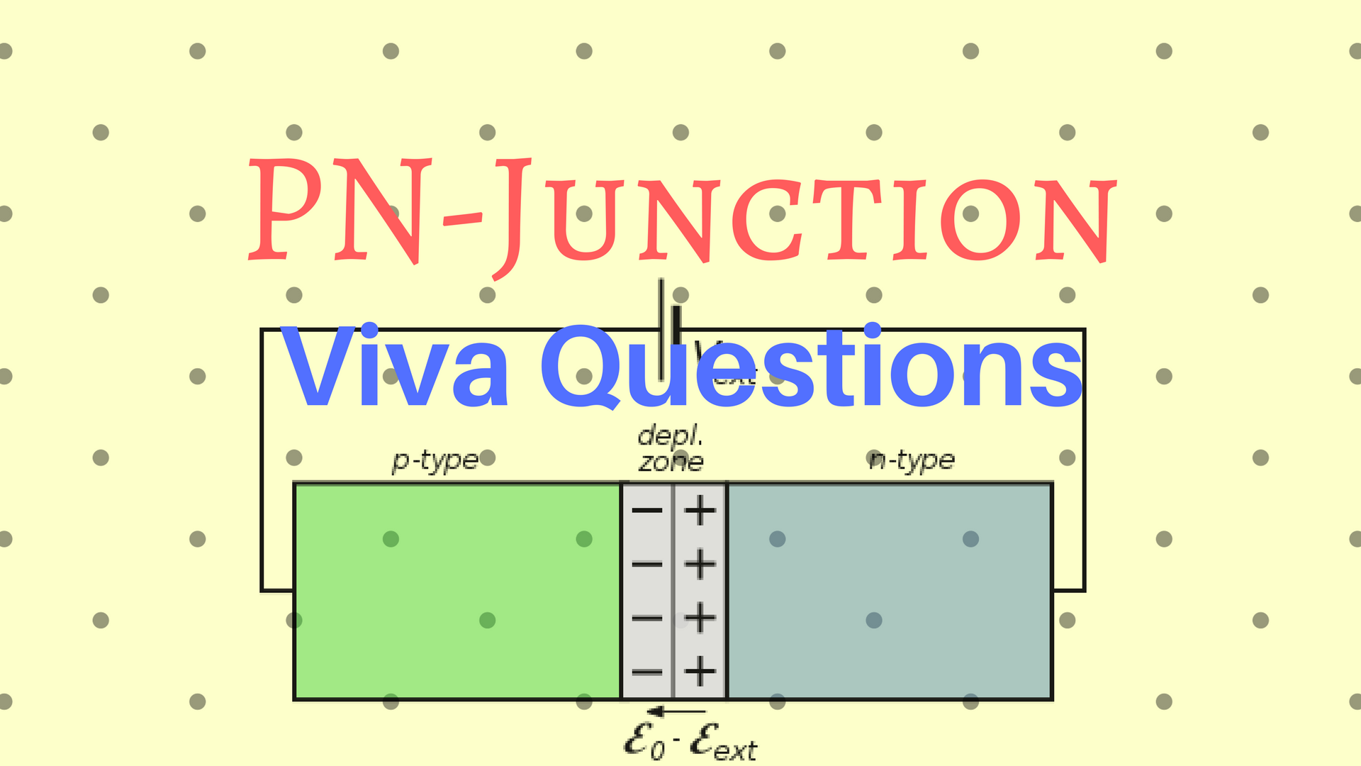
2. How depletion region is formed in the PN junction?
3. What is leakage current?
4. What is break down voltage?
5. What is an ideal diode? How does it differ from a real diode?
6. What is the effect of temperature in the diode reverse characteristics?
7. What is cut-in or knee voltage? Specify its value in case of Ge or Si?
8. What are the difference between Ge and Si diode.
9. What is the capacitance formed at forward biasing?
10. What is the relationship between depletion width and the concentration of impurities?
11. How does the I-V characteristic of a heavily doped diode differ from that of a lightly
doped diode? Why does the I-V characteristics differ?
12. For any diode, how does the I-V characteristic change as temperature increases?
13. For the same doping concentration, how does the I-V characteristic of a wide band gap
(Eg) semiconductor compare to a narrow band gap semiconductor (say GaAs vs. Si)?
I’m a physicist specializing in computational material science with a PhD in Physics from Friedrich-Schiller University Jena, Germany. I write efficient codes for simulating light-matter interactions at atomic scales. I like to develop Physics, DFT, and Machine Learning related apps and software from time to time. Can code in most of the popular languages. I like to share my knowledge in Physics and applications using this Blog and a YouTube channel.
Please give answers to the above questions
please give answers to the above questions